Yet some more schematics of power amps
Some well known schematics which was widely used by manufacturers was described in:
"The influence of schematics on
power amplifier parameters". Here some interesting schemes are added. So it is a
somewhat "part 3" of that article. The next parts may appear: the mankind has created
much!
All schemes are simulated with Electronics WorkBench (EWB) and are not for immediate
implementation in real projects, but is a kind of mental pabulum.
All amps are non-inverting (as before), though inverting amps have some advantages.
As before every subsequent scheme is a result of evolution of the previous one or
some of the previous. The amplification factor of all schemes with negative feedback (NFB)
is 100/3+1=34.33.
The power source voltages are+_50 V, except the third one, where they are +_30 V.
the two differential stages amp
There can be some other schemes with two differential stages.
The first stage is the differential pair with cascode. The second stage is a differential
pair with split current source and current mirror. This topology has 4 times more gain, than
the second amp from "The influence of schematics on power amplifier parameters. Part 1" -
the amplifier with current source voltage amplifier stage. The second stage can provide
the maximum amplitude load current equal to double collector current of each transistor
in the pair. That means that the collector current can be lower than in a stage with single
transistor (accordingly the power dissipation is lower too). The scheme without cascodes in
both stages is possible too.
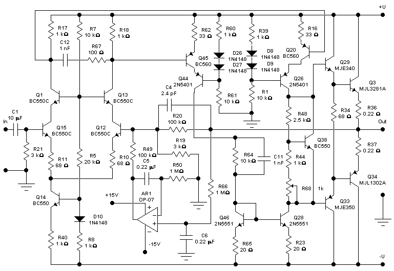
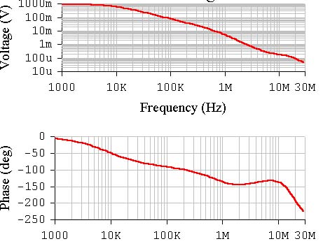
The amplitude versus frequency graph of the amp with open NFB loop:
The input voltage amplitude is 1 mV.
The open loop gain is higher than 10 000. The open loop bandwidth of the amp is
higher than 30 kHz. And it is good!
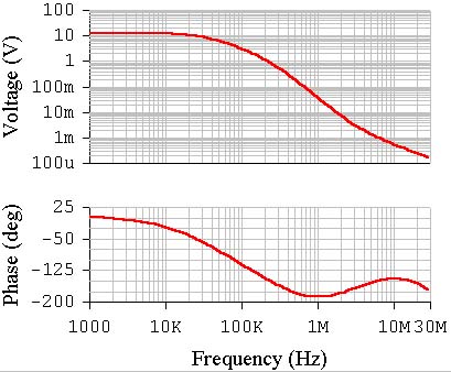
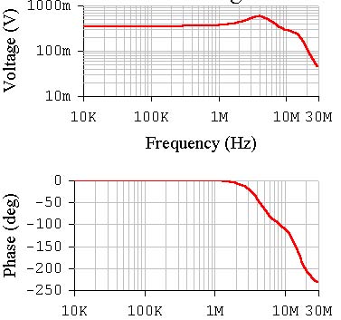
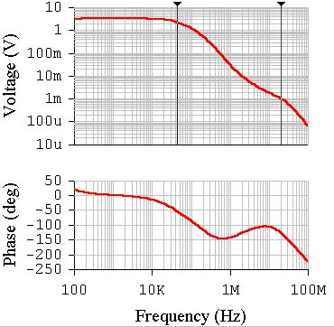
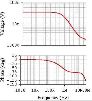
The amplitude and phase versus frequency of this amp with NFB graphs are shown below:
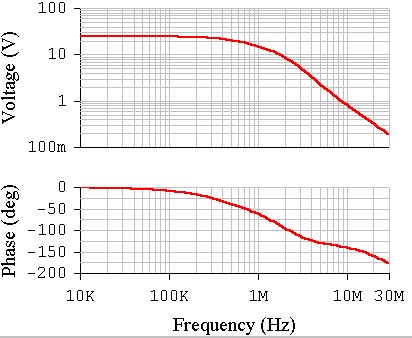
The amp is stable as can be seen.
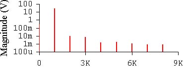
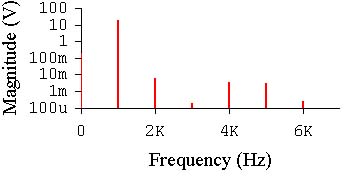
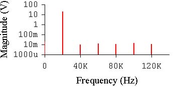
The THD at the amplitude input voltage 0.7 V (approximately 40 W at 8 ohms load) is
0.043% (1 kHz) and 0.16% (20 kHz). The output transistors quiescent current is
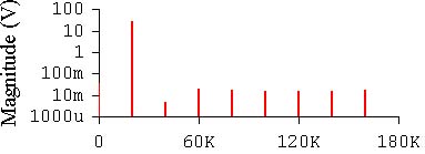
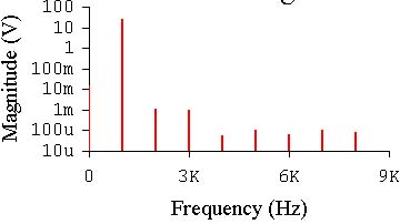
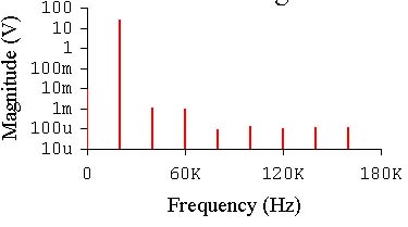
about 140 mA. The harmonics spectrum for both cases are shown below:
the three differential stages schematics
Such schematics was used by "Electrocompaniet" and was designed by Otala
in 1973. It must be mentioned that all transistor schematics was designed in
seventies. The interesting site of the former employee of this Scandinavian company
with schematics:
www.home.sol.no/~tersands/schematics.htm
see: [LINKS].
A somewhat like schematics was used in ВА-6000 amplifier by Fischer at the beginning
of the eighties.
A hybrid of the two amps is shown here. I couldn't make the amp stable as was
in the Electrocompaniet amp so the 2 more
frequency compensation capacitors are used in the third stage. The DC servo amp and
NFB circuit capacitor are not shown simply because of image space limits.
The amplitude versus frequency graph of the amp with open NFB loop:
The amplitude input voltage is 10 uV. The amp is relatively stable. The open NFB loop
gain is a little less 100 000! The rolloff of the gain graph is at 7 kHz. If
the overall gain is made less the gain graph can be made flat till 20 kHz or more
(as it was done by Electrocompaniet). The THD will be slightly higher than.
The amplitude and phase versus frequency of this amp with NFB graphs are shown below:
As can be seen from the graph, the amp is relatively stable. It would be hard to achieve
stability in a real project.
The THD at the input voltage 0,7 V (40 W at Rload=8 ohms) is 0.0055% and 0.0054% at 1
and 20 kHz respectively. This is the result of a three stage design and the lead correction.
The output transistors quiescent current is about 140 mA.
And what is the THD at 100 kHz? 0.0056%!
The harmonics spectrum for 1 and 20 kHz are shown below:
It must be mentioned that using the lead correction we can dramatically increase the frequency
range and reduce THD at high frequencies. All the previous amps were subject to high THD at
20 kHz.
another two differential stages scheme with uncomplementary output
emitter-follower
This topology differs from everything that was described before. It was useful when
high power complementary transistor pairs were scarce. So the special second
differential stage made it possible to use only npn devices as output and even driver stage!
The scheme is thermally unstable. So it can not be implemented "as is".
The means of eliminating this shortcoming - see below.
The first stage was described before. A simple differential stage with resistive
load can be used too. The second stage is a resistive load differential pair but
the load resistors are connected to different rails: the output and negative power
supply rail. The Q44 may be thrown away. It makes the collector voltages of Q45
and Q20 equal when there is no signal. The second stage has low gain because
the load resistors R23, R73 can not not have large values, which are determined by
two Ube of output pairs. Using power MOSFETs can make possible higher values resistors.
The amplitude versus frequency graph of the amp with open NFB loop:
The amplitude input voltage is 1 mV. The overall open loop gain is only 3250.
The amplitude graph is flat till 44 kHz (-3dB).
The amplitude and phase versus frequency of this amp with NFB graphs are shown below:
The amp is stable.
THD at 0.5 V amplitude input voltage are 0.041 at 1 kHz and 0.15 at 20 kHz.
The quiescent current of the output transistors is 167 mA. Without Q44 these figures
are 0.06 and 0.14 respectively.
The pictures below show the harmonics spectrum at 1 and 20 kHz:
And a few words about thermal non-stability of this amp.
This is caused by two reasons. First: the standing current of the second differential
stage is defined only by low value resistor R68. This is a common defect of the two
differential stages topology. This drawback can be overcome by feeding it from the more
high voltage source of positive polarity (it may be +40 V). In this case transistor
current source can be used instead of resistor.
Having eliminated the temperature instability of the second stage we did not solve
the whole problem. It can be seen that there are no components that provide the
output transistors quiescent current thermal stability. That brings to their
self heating. To stabilize the current the currents of the second or even first
stages are to be controlled according to the output stage devices temperature.
This leads to the changing of operation conditions of all (in the second case)
or almost all transistors of voltage amplifier stages. So their frequency
parameters can also change.
The amp is suitable for class A operation of the output transistors.
In that case we need to stabilize the mean current by some servo scheme.
As it was pointed out the little gain of the second stage and of the whole amp
is determined by low resistance of the second stage load. The resistance of R23=R73
is equal to sum of emitter-base voltages of the output pair divided by the half of
second stage standing current. Mosfets have the Ugs (gate - source voltage) larger
than the sum of emitter-base voltages of the output bipolar pair and the second stage
gain may be higher. Such schematics can be found on the Australian site:
": www.vision.net.au
/~anthony - "The D.I.Y. amplifier page"
And in conclusion let us switch the amp into A class mode (the output quiescent current
is 5.09 A) by making R23=R73=470 ohms. C12=300 pF, the two new frequency compensation
20 pF capacitors from base to collectors of Q45 ang Q20.
The THD at 1 kHz lowered to 0.017% but at 20 kHz the THD are 0.17%. In reality
minimum two pairs of output transistors should be used to handle 5 amperes at 30 volts.