The influence of schematics on power amplifier parameters. Part 2

     In the first part of the article: " The influence of schematics..." the "asymmetric" amplifiers were discussed. The inverted commas are present because these schemes are not usually called in such a way. Here the "symmetric" schematics is discussed. In the inverted commas are here again because, though they are called so, absolute symmetry is hard to achieve even if the transistors are "complementary". If transistors with equal H21e and even equal emitter-base voltage can be selected from a pile a great scatter of transition frequencies between specimen still exists. But such schemes look good, they are comprehensible and have symmetrical clipping. The output stage was in fact symmetric in all schemes (we do not discuss quasi complementary output), that is why the word "symmetry" is about voltage amplifier.
     The DIY amps with such schematics were popular in Russia in the eighties. Some descriptions and projects were published in the "Radio" magazine.
     In the input stages another models of transistors are used. This was caused by the fact that the SPICE model BC546 simply didn't work correctly at the time this article was prepared. But this doesn't make the results not comparable. BC327-BC337 are almost the same as BC546-BC556.
     I apologize for the fact that some lables on the schematic diagrams are not readable. All the elements are the same in different schemes, for instance all the diodes are 1N4148.
    

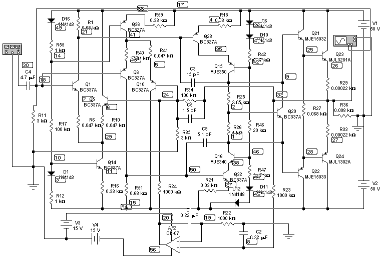
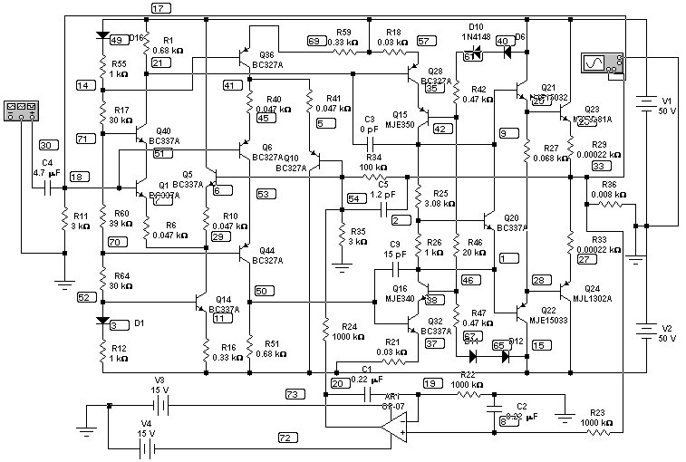
symmetrical scheme with resistive first stage load and cascode second stage.

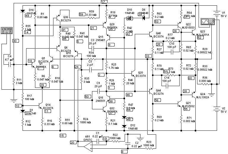
     This scheme is a hybrid of the second and the fifth schemes from part one. We can expect twice as high open loop gain as the second scheme from part 1 and the same high slew rate as in the fifth.
     At the resistor values shown the first stage quiescent current is 3.53 mA, the second - 20.4 mA, the output power transistors - 150 mA.
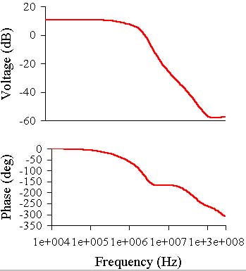
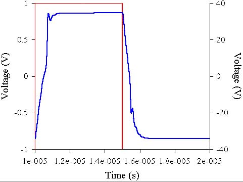
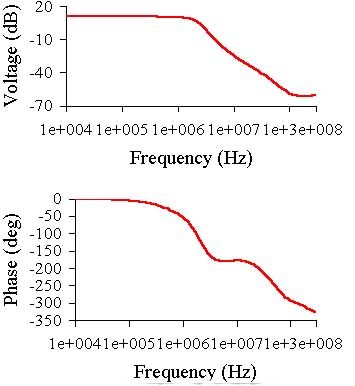
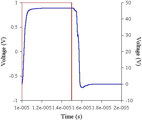
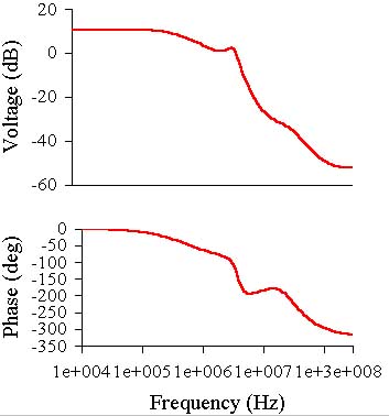
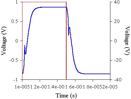
     The gain and phase versus frequency graphs and 100 kHz square wave at the output are shown below (the output signal here and further is blue):

     The stability of the amp is provided by standard frequency compensation (C3, C9 - two capacitors instead of one in the "asymmetric" design) and the lead correction (C5).
     To make this amp stable C3 and C9 have different values, this illustrates that symmetry is virtual. Sure the 15 pF caps can be used in both cases. The pips at both fronts of the square impulse can be not because the amp has no absolute stability but because of crossover distortions .
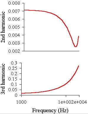
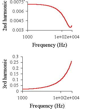
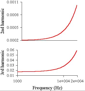
     The amp shows the same level of harmonics as the second scheme in part 1. That means that considerable schematics complexity gave little improvement.
     But the symmetric input topology has important feature: the base currents reciprocally compensate (if the pnp and npn transistors are matched by H21e). As a result the current through R11 doesn't flow and there is no voltage drop on it (almost). So the resistors at the inverting and non-inverting inputs can be not equal. This is true for all schematics below.


     Nodes voltages:
     Node    Voltage
1      -1.1493
2      -0.6681
3      -49.045
4      49.388
5      0.40385
6      -0.41246
7      -0.41303
8      -0.00078197
9      1.1239
10     -48.436
11     -48.862
14     48.433
15     -50
17     50
18     -0.0048703
19     -0.00078206
20     0.19474
21     48.905
24     -0.0043124
25     0.58154
26     0.033123
27     -0.033123
28     -0.6444
29     -0.49346
30     0
33     9.323e-008
35     47.104
37     -49.387
38     -47.1
39     49.292
40     48.585
41     0.4847
42     46.445
43     -49.294
44     -48.588
45     0.40358
46     -46.485
49     49.39
50     -48.905
51     15
55     48.859
56     -15

Amp with cascodes in both stages

    
     This amp must have a little higher slew rate than the previous one and as it has the same gain the distortions can no be expected to be lower.
     At the revalues values shown the first stage quiescent current is 3.48 mA, the second - 19.7 mA, the output power transistors - 152.5 mA (almost the same as in the previous case).
     The gain and phase versus frequency graphs and 100 kHz square wave at the output are shown below:


     The square impulse looks better and the gain begins to drop after 1 mHz while the previous one did so at lower frequency. The amp is more stable than the previous.
     Then the second and third harmonics graphs:
     As I said the distortions are not lower than in the previous case.


     And the nodes voltages:
Node    Voltage
1      -1.1502
2      -0.66994
3      -49.034
5      0.40369
6      -0.41459
7      -0.41938
8      -0.00078277
9      1.1249
11     -48.85
14     48.419
15     -50
17     50
18     -0.005751
19     -0.00078207
20     -0.20094
21     48.928
25     0.58246
26     0.033589
27     -0.03359
28     -0.64521
29     -0.49851
30     0
33     -7.1591e-007
35     47.101
37     -49.409
38     -47.096
40     49.292
41     0.48784
42     46.443
45     0.40813
46     -46.482
48     0
49     49.39
50     -48.928
51     18.552
52     -48.424
53     -18.61
54     -0.0055204
57     49.41
61     48.585
65     -49.294
67     -48.588
69     48.846
70     -19.021
71     18.963
72     -15
73     15

The three stage voltage amplifier amp

     This is the only scheme here where the third stage has voltage gain (though some other schematics are possible). This makes possible to make overall open loop gain higher. Also the first (and the second) stages can have lower supply voltages (and transistors with lower Uceo can be used). Here nothing of this is done - it wouldn't change the results of our analysis.
     What was done: the second stage current is lower: 7 mA, which made possible to use higher transition frequency and voltage but low power transistors: 2N5551 and 2N540currenturerent can be lower because the output stage consists now triples. It's maximum input current is now a hundred times lower than in all previous schemes. It must be pointed out that the use of BC327A - BC337A as Q40 è Q44 is impossible in practical schematics, they do not meet the Uceo and Po requirements. BF422, BF423 would be enough. But the result of our analysis will be adequate with the used models.
     The third stage voltage gain is three.
     The three stage amp needs more frequency compensation elements (C10 and C14 in our case). R64, R71 give better thermal stability.
     At the revalues values shown the first stage quiescent current is 4.18 mA, the second - 6.86 mA, the output power transistors - 145.9 mA
     The gain and phase versus frequency graphs and 100 kHz square wave at the output are shown below:


     The crossover distortions can be seen on the square impulse. Amplitude (gain) versus frequency graph doesn't show anything good.
     Next: second and third harmonics graphs in the 1-20 kHz range:

     It can be easily seen that distortions a 10 times less than the previous amp and are even better than that of the amp with emitter-follower between the first and second stages from part 1.


     Node voltages:
Node    Voltage
1      -0.66842
2      -0.21632
3      -49.045
4      49.314
5      0.40343
6      -0.41289
7      -0.41315
8      -0.00146
9      0.64219
10     -48.436
11     -48.862
14     48.433
15     -50
17     50
18     -0.0049408
19     -0.0014
20     -0.00075252
21     48.86
24     -0.0047918
25     0.21859
26     0.58081
28     -0.64106
29     -0.49374
30     0
33     0.00074
35     44.694
37     -49.313
38     -48.858
39     49.292
40     48.584
41     0.48443
42     44.018
43     -49.292
44     -48.584
45     0.40346
46     -48.127
48     0
49     49.39
50     -48.859
51     49.911
52     0.033236
53     49.391
54     -0.24175
55     -49.901
56     -49.34
59     48.859
60     -0.031002
     This scheme is used for the illustration of the influence of the output stage quiescent current on the amplifier parameters:"
The influence of quiescent bias current of the output stage on the amplifier parameters ". The other symmetrical topologies are possible. For instance the third stage can be as described in "Curious thing about Bragin's amplifier". The emitter-followers between the first and second stages are possible.
     I have simulated interesting symmetric scheme:
symmetrical amplifier without differential first stage .

conclusions

     If one compares by what the last schematic diagram differs from the first, he can see that the last one has two times more transistors and passive components too. That means it is much more complex. But if one looks at the real amps built according to this schematics, he can hardly see the difference: the PCB is only slightly larger (not twice larger). The most costly and massive components of the amp are mains transformer, capacitors of the power supply and power transistor heat sinks. Ten low power transistors cost 50 cents or 1$ just as one output transistor. The more complex schematics give better characteristics. So they deserve consideration. One has only understand how it all works and what he gets making the given alterations in schematics.
     After the whole article was ready I made the EWB to "measure" the THD (total harmonic distortions) of all schemes. The program sometimes gives strange results (EWB V5.0), but the whole picture looks like real life in general. THD are "measured" at 1 and 20 kHz at 1.5 and 72 watts power: the input voltages are: 0.1 and 0.7 V. The results are in the table:
Name F=1 kHz F=20 kHz
Power 1.5 Âò Power 72 Âò Power 1.5 Âò Power 72 Âò
Schematics with a bootstrap 1.25 32.6 - -
Amplifier with current source voltage amplifier stage 0.022 0.14 0.034 0.28
0.011 0.042 0.010 0.10
Amp with emitter-follower in the second stage 0.017 0.0097 0.0398 0.22
Amp with cascode in the second stage 0.0089 0.013 0.069 0.25
Amp with cascodes both stages 0.029 0.019 0.054 0.41
Symmetrical scheme with resistive first stage load and cascode second stage 0.0046 0.014 0.071 0.15
Symmetrical amp with cascodes in both stages 0.065 0.038 0.011 0.24
The three stage voltage amplifier amp 0.096 0.0017 0.033 0.31

     As can be seen the scheme with emitter-follower has very low THD, like the next two. Though cascode in the first stage gave nothing. Symmetrical schemes also have low THD. And in this case nothing was gained by adding cascode to the first stage. The three stages topology showed almost no advantage ower the two stage one except the high power distortions at 1 kHz. Proper frequency compensation and optimization of resistors can make it better.
    

To part one