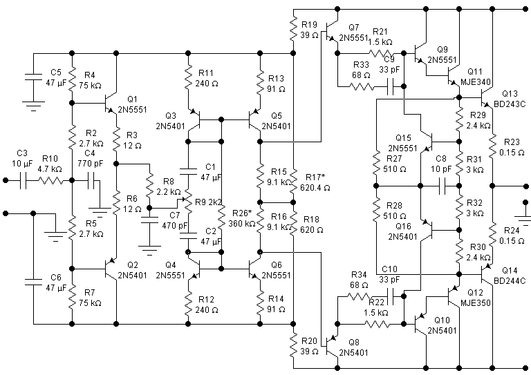
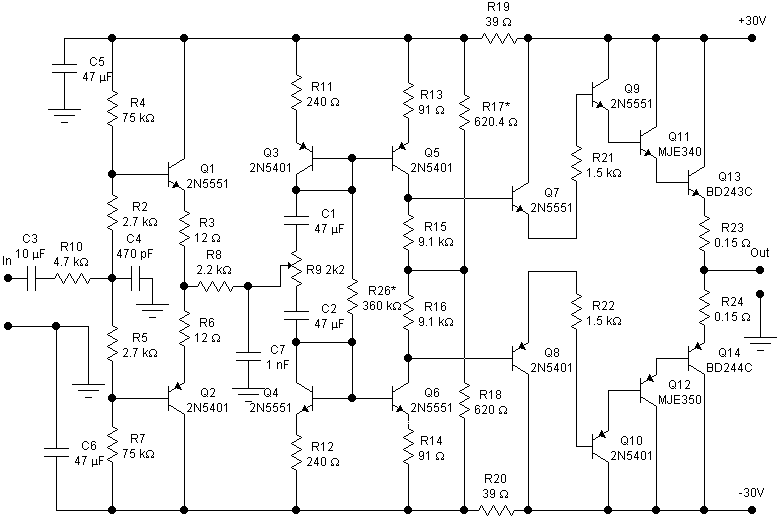
| Output Power into 8 Ohms | 120 Watts |
| Output Power into 4 Ohms | 240 Watts |
| Output Power into 3 Ohms | 300 Watts |
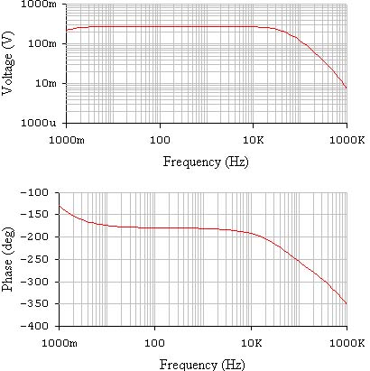
| Frequency Response +-3dB | DC-500.000 Hz |
| Phase shift @ 20.000Hz | max. 2 deg. |
| THD -3dB | 0,0017% |
| Peak Current 1 mS | 46 Amperes |
| Output Impedance | 150 mOhm |
| Damping Factor (50 - 15.000 Hz) | 53 |
| Equivalent input noise | 20 uV RMS |
| Signal / Noise Ratio | min. 110 dBA |
| Uin ampl (mV) | Uout ampl (V) | P (W) | THD (1 kHz) (%) | THD (20 kHz) (%) |
| 100 | 5.14 | 1.65 | 0.251 | 0.383 |
| 200 | 10.28 | 6.6 | 0.242 | 0.357 |
| 300 | 15.42 | 14.9 | 0.254 | 0.335 |
| 400 | 20.56 | 26.4 | 0.297 | 0.335 |
| 500 | 25.7 | 41.3 (-3 dB) | 0.377 | 0.372 |
| 600 | 30.84 | 59.4 | 0.498 | 0.501 |
| 700 | 35.98 | 81 (0 dB) | 0.673 | 0.700 |
| 750 | 38.55 | 92.9 | 2.53 (clipping) | 2.55 |
| Uin ampl (V) | THD1 (1 kHz) (%) | THD1 (20 kHz) (%) | THD2 (1 kHz) (%) | THD2 (20 kHz) (%) |
| 1 | 0.709 | 1.93 | 0.636 | 1.91 |
| 2 | 0.448 | 2.97 | 0.425 | 3.29 |
| 3 | 0.89 | 2.4 | 1.65 | 3.77 |
| 4 | 1.16 | 1.93 | 3.85 | 5.19 |
| 5 (Pout=22W, 8 Ohm) | 1.25 | 1.73 | 5.89 | 6.99 |
| 6 | 5.41 | 3.19 | - | - |